UVM Partners with GlobalFoundries, Department of Education on New Semiconductor Lab
Source: VermontBiz
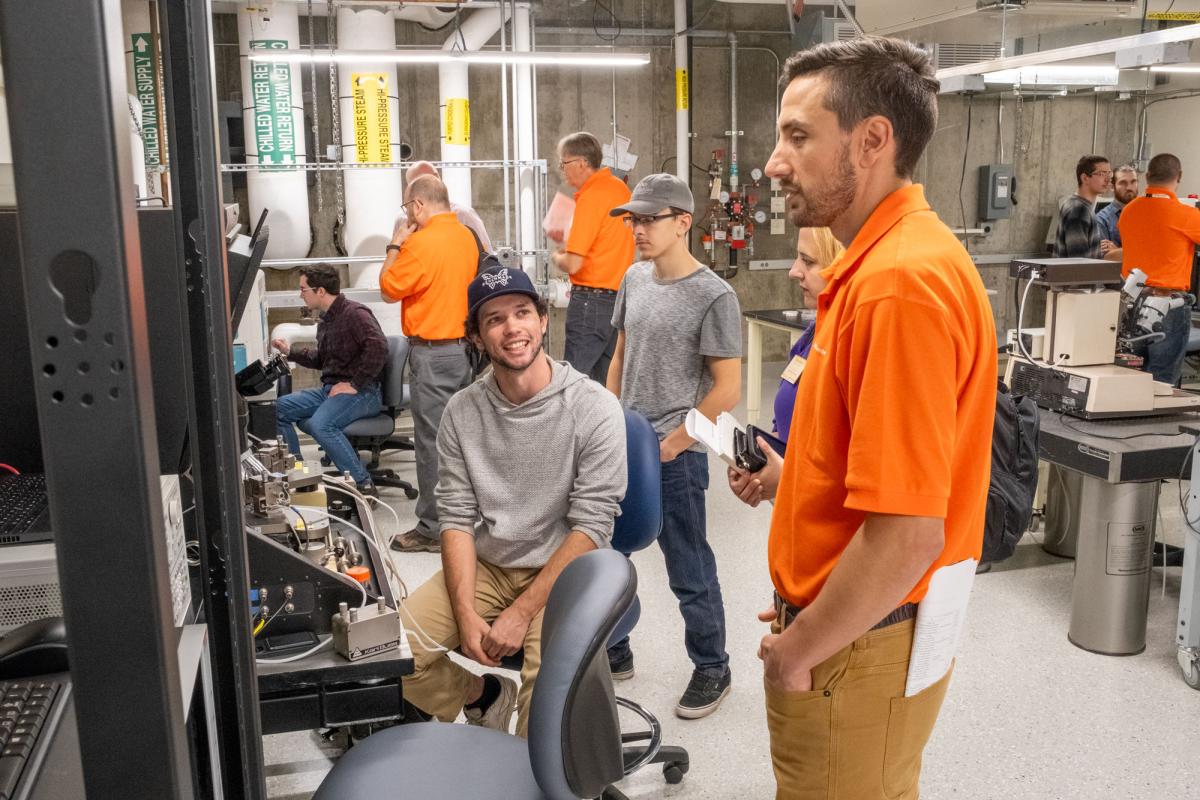
An innovative Device Characterization Lab opened at the University of Vermont, made possible by a partnership between UVM’s College of Engineering and Mathematical Sciences (CEMS) and GlobalFoundries (GF).
The only educational semiconductor lab in the state, the new lab heralds an essential phase of the ongoing initiative to prepare students to work in the rapidly expanding field. The facility features a suite of scientific testing and analysis equipment donated by GF.
“Our strategic partnership with GF continues to build on our shared commitment to developing a highly skilled workforce that positions Vermont as a leader in semiconductor development and manufacturing,” said Linda Schadler, dean of CEMS. “This cutting-edge facility is the first of its kind in Vermont and will provide a unique educational experience for our students.”
The seed of the project was planted last fall when the U.S. Department of Education (DoE) awarded UVM $2.6M to develop and implement expanded educational opportunities in semiconductor technology.
With the funding in place, a team of CEMS faculty members collaborated with their colleagues at GF to design an Undergraduate Certificate in Semiconductor Engineering and Physics (UCSEP) as part of the new enhanced semiconductor curriculum. The 17-credit certificate prioritizes the hands-on experience that the new Device Characterization Lab will provide.
“It’s unusual for undergraduate students to be able to get their hands on state-of-the-art probers and parameter analyzers—instruments that would normally be found in an industrial or a research laboratory,” said Matt Gallagher at UVM, who has helped coordinate the equipment donation and is teaching the first course in the lab this fall.
“Development in critical areas such as this are foundational to UVM’s identity as a premier research institution,” said Kirk Dombrowski, Vice President of Research at UVM. “Hands-on learning that originates in this lab will be carried forth into the workforce by our students and put to use for employers such as GF, further strengthening our shared positions as leaders in innovation.”
As the basic building blocks for computing and communications devices, semiconductors are embedded into nearly every facet of our modern lives – from automotive and telecommunications technology to national defense systems.
The scientific equipment donated by GF provides students and researchers with the opportunity to conduct semiconductor failure analysis and characterization—the process by which a material’s properties are analyzed and measured.
The new lab joins the University’s existing clean room as part of a robust hands-on opportunity for students to learn on the same equipment being used in semiconductor manufacturing facilities known in the industry as fabrication plants, or fabs. A 13-credit graduate-level certificate is also on the horizon beginning in fall 2024 during which students will travel to the GF Vermont facility and have access to their state-of-the-art characterization laboratories.
A video about the new facility and program can be viewed here: https://go.uvm.edu/gfpartnership


